

DATE - 2023/08/28
CET N-Channel Enhancement Mode Field Effect Transistor

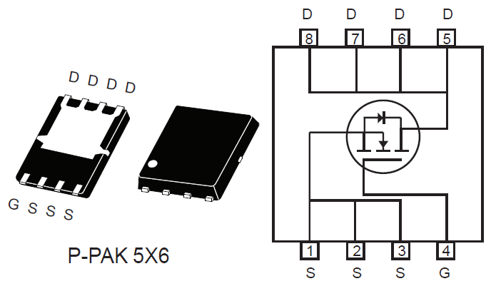
CEZC3062
N-Channel Enhancement Mode Field Effect Transistor
FEATURES
•30V, 48A, RDS (ON) =6.7 mW @VGS =10V.
RDS (ON) =8.7 mW @VGS =4.5V.
•Super high dense cell design for extremely low RDS(ON).
•High power and current handing capability.
•Pb-free lead plating ; RoHS compliant.
•Surface mount Package.
| Parameter | Symbol | Limit | Units |
| Drain-Source Voltage | VDS | 30 | V |
| Gate-Source Voltage | VGS | ±20 | V |
| Drain Current-Continuous | ID@RθJC | 48 | A |
| Drain Current-Continuous | ID@RθJA | 15 | A |
| Drain Current-Pulsed a | IDM@RθJC | 192 | A |
| Drain Current-Pulsed a | IDM@RθJA | 60 | A |
| Maximum Power Dissipation | PD | 25 | W |
| Operating and Store Temperature Range | TJ,Tstg | -55 to 150 | C |


CEZ2R04
N-Channel Enhancement Mode Field Effect Transistor
FEATURES
•40V, 121A, RDS (ON) =2.4 mW @VGS =10V.
RDS (ON) =3.5 mW @VGS =4.5V.
•Super high dense cell design for extremely low RDS(ON).
•High power and current handing capability.
•Pb-free lead plating ; RoHS compliant.
•Halogen Free.
•Surface mount Package.
| Parameter | Symbol | Limit | Units |
| Drain-Source Voltage | VDS | 40 | V |
| Gate-Source Voltage | VGS | ±20 | V |
| Drain Current-Continuous | ID@RθJC | 121 | A |
| Drain Current-Continuous | ID@RθJA | 40 | A |
| Drain Current-Pulsed a | IDM@RθJC | 484 | A |
| Drain Current-Pulsed a | IDM@RθJA | 160 | A |
| Maximum Power Dissipation | PD | 56 | W |
| Single Pulsed Avalanche Energy d | EAS | 312.5 | mJ |
| Single Pulsed Avalanche Current d | IAS | 25 | A |
| Operating and Store Temperature Range | TJ,Tstg | -55 to 150 | C |
CEZ03R04
N-Channel Enhancement Mode Field Effect Transistor
FEATURES
•40V, 103A, RDS (ON) =2.9 mW @VGS =10V.
RDS (ON) =4.2 mW @VGS =4.5V.
•Super high dense cell design for extremely low RDS(ON).
•High power and current handing capability.
•Pb-free lead plating ; RoHS compliant.
•Halogen Free.
•Surface mount Package.
| Parameter | Symbol | Limit | Units |
| Drain-Source Voltage | VDS | 40 | V |
| Gate-Source Voltage | VGS | ±20 | V |
| Drain Current-Continuous | ID@RθJC | 103 | A |
| Drain Current-Continuous | ID@RθJA | 30 | A |
| Drain Current-Pulsed a | IDM@RθJC | 412 | A |
| Drain Current-Pulsed a | IDM@RθJA | 120 | A |
| Maximum Power Dissipation | PD | 56 | W |
| Single Pulsed Avalanche Energy d | EAS | 80 | mJ |
| Single Pulsed Avalanche Current d | IAS | 40 | A |
| Operating and Store Temperature Range | TJ,Tstg | -55 to 150 | C |
N-Channel Enhancement Mode Field Effect Transistor
FEATURES
•100V, 81A, RDS (ON) =5.5 mW @VGS =10V.
RDS (ON) =8.7 mW @VGS =4.5V.
•Super high dense cell design for extremely low RDS(ON).
•High power and current handing capability.
•Pb-free lead plating ; RoHS compliant.
•Halogen Free.
•Surface mount Package.
| Parameter | Symbol | Limit | Units |
| Drain-Source Voltage | VDS | 100 | V |
| Gate-Source Voltage | VGS | ±20 | V |
| Drain Current-Continuous | ID@RθJC | 81 | A |
| Drain Current-Continuous | ID@RθJA | 20 | A |
| Drain Current-Pulsed a | IDM@RθJC | 324 | A |
| Drain Current-Pulsed a | IDM@RθJA | 80 | A |
| Maximum Power Dissipation | PD | 83 | W |
| Operating and Store Temperature Range | TJ,Tstg | -55 to 150 | C |
CEZ07C04L
N-Channel Enhancement Mode Field Effect Transistor
FEATURES
•40V, 296A, RDS (ON) =0.7 mW @VGS =10V.
RDS (ON) =1.1 mW @VGS =4.5V.
•Super high dense cell design for extremely low RDS(ON).
•High power and current handing capability.
•Pb-free lead plating ; RoHS compliant.
•Halogen Free.
•Surface mount Package.
| Parameter | Symbol | Limit | Units |
| Drain-Source Voltage | VDS | 40 | V |
| Gate-Source Voltage | VGS | ±20 | V |
| Drain Current-Continuous | ID@RθJC | 296 | A |
| Drain Current-Continuous | ID@RθJA | 72 | A |
| Drain Current-Pulsed a | IDM@RθJC | 1184 | A |
| Drain Current-Pulsed a | IDM@RθJA | 288 | A |
| Maximum Power Dissipation | PD | 104 | W |
| Operating and Store Temperature Range | TJ,Tstg | -55 to 150 | C |
CEZ09C04H
N-Channel Enhancement Mode Field Effect Transistor
FEATURES
•40V, 222A, RDS (ON) =1.05 mW @VGS =10V.
•Super high dense cell design for extremely low RDS(ON).
•High power and current handing capability.
•Pb-free lead plating ; RoHS compliant.
•Halogen Free.
•Surface mount Package.
| Parameter | Symbol | Limit | Units |
| Drain-Source Voltage | VDS | 40 | V |
| Gate-Source Voltage | VGS | ±20 | V |
| Drain Current-Continuous | ID@RθJC | 222 | A |
| Drain Current-Continuous | ID@RθJA | 60 | A |
| Drain Current-Pulsed a | IDM@RθJC | 888 | A |
| Drain Current-Pulsed a | IDM@RθJA | 240 | A |
| Maximum Power Dissipation | PD | 83 | W |
| Operating and Store Temperature Range | TJ,Tstg | -55 to 150 | C |
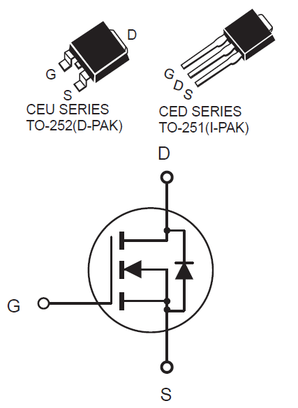
CED22N60SF/CEU22N60SF
N-Channel Enhancement Mode Field Effect Transistor
With Fast Body Diode
With Fast Body Diode
FEATURES
•650V@TJ max, 19A, RDS(ON) =134mW @VGS =10V.
•Super high dense cell design for extremely low RDS(ON).
•High power and current handing capability.
•Pb-free lead plating ; RoHS compliant.
•Halogen Free.
•Fast reverse recovery time.
•TO-251 & TO-252 package.
•TO-251 & TO-252 package.
| Parameter | Symbol | Limit | Units |
| Drain-Source Voltage | VDS | 600 | V |
| Gate-Source Voltage | VGS | ±30 | V |
| Drain Current-Continuous @ TC = 25 C @ TC = 100 C |
ID | 19 12 |
A |
| Drain Current-Pulsed a | IDM | 76 | A |
| Maximum Power Dissipation @ TC = 25 C - Derate above 25 C |
PD | 125 1 |
W W/ C |
| Single Pulsed Avalanche Energy d | EAS | 81 | mJ |
| Single Pulsed Avalanche Current d | IAS | 4.5 | A |
| Operating and Store Temperature Range | TJ,Tstg | -55 to 150 | C |
CEZ25R06L
N-Channel Enhancement Mode Field Effect Transistor
FEATURES
•60V, 118A, RDS (ON) =2.5 mW @VGS =10V.
RDS (ON) =4.1 mW @VGS =4.5V.
•Super high dense cell design for extremely low RDS(ON).
•High power and current handing capability.
•Pb-free lead plating ; RoHS compliant.
•Halogen Free.
•Surface mount Package.
| Parameter | Symbol | Limit | Units |
| Drain-Source Voltage | VDS | 60 | V |
| Gate-Source Voltage | VGS | ±20 | V |
| Drain Current-Continuous | ID@RθJC | 118 | A |
| Drain Current-Continuous | ID@RθJA | 30 | A |
| Drain Current-Pulsed a | IDM@RθJC | 412 | A |
| Drain Current-Pulsed a | IDM@RθJA | 120 | A |
| Maximum Power Dissipation | PD | 83 | W |
| Operating and Store Temperature Range | TJ,Tstg | -55 to 150 | C |