圖片僅供參考
| FLYiNG 零件編號 | ICCD4066BETI |
| FLYiNG 散料庫存 | 電洽/Contact |
| FLYiNG 標準包裝庫存 | 電洽/Contact |
| 製造商/品牌商 | TEXAS INSTRUMENTS |
| 製造商/品牌商零件編號 | CD4066BE |
| 說明 | IC CD4066BE PDIP-14 TI |
| 無鉛狀態 / RoHS 指令狀態 | 符合 ROHS3 指令 |
| 散裝數量 | NTD 單價 / PCS |
| 1~9 | 18 |
| 10~99 | 13 |
| 積體電路類型 | CMOS Quad Bilateral Switch |
| 原廠料號 | CD4066BE |
| 通道數 | 4 Channel |
| 配置 | 4 x SPST |
| 電源電壓 | 3V ~ 18V |
| 雙電源電壓 | +/- 7.5V |
| 最大啟動時間 | 30ns |
| 最大關閉時間 | 30ns |
| 工作溫度 | -55°C ~ 125°C |
| 封裝/外殼 | PDIP-14 |
| 標準包裝數量 | 25/Tube |
CD4066B CMOS Quad Bilateral Switch
Features
The CD4066B device is a quad bilateral switch intended for the transmission or multiplexing of analog or digital signals. It is pin-for-pin compatible with the CD4016B device, but exhibits a much lower on-state resistance. In addition, the on-state resistance is relatively constant over the full signalinput range.
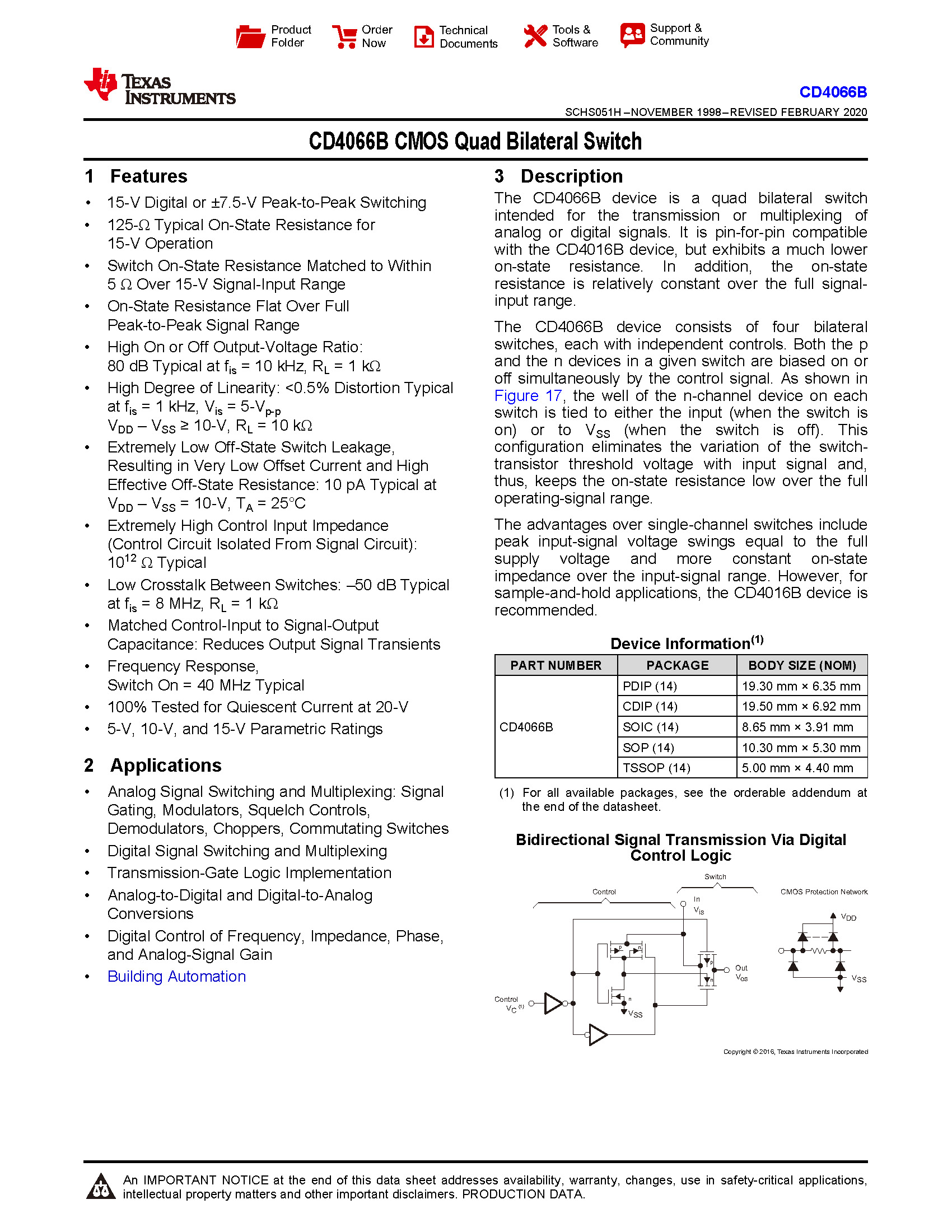
The CD4066B device consists of four bilateral switches, each with independent controls. Both the p and the n devices in a given switch are biased on or off simultaneously by the control signal. As shown in Figure 17, the well of the n-channel device on each
switch is tied to either the input (when the switch is on) or to VSS (when the switch is off). This configuration eliminates the variation of the switchtransistor threshold voltage with input signal and, thus, keeps the on-state resistance low over the full operating-signal range.
The advantages over single-channel switches include peak input-signal voltage swings equal to the full supply voltage and more constant on-state impedance over the input-signal range. However, for sample-and-hold applications, the CD4016B device is recommended.
CD4066B CMOS 四路雙邊開關
特徵
CD4066B 器件是一個四路雙向開關,用於模擬或數字信號的傳輸或多路復用。它與 CD4016B 器件引腳對引腳兼容,但導通電阻要低得多。此外,通態電阻在整個信號輸入範圍內相對恆定。
CD4066B 設備由四個雙邊開關組成,每個開關都有獨立的控制。給定開關中的 p 和 n 器件都由控制信號同時偏置開或關。如圖 17 所示,每個 n 溝道器件的阱
開關連接到輸入(當開關打開時)或 VSS(當開關關閉時)。這種配置消除了開關晶體管閾值電壓隨輸入信號的變化,因此在整個工作信號範圍內保持低通態電阻。
與單通道開關相比,其優勢包括峰值輸入信號電壓擺幅等於全電源電壓,以及在輸入信號範圍內更恆定的導通狀態阻抗。但是,對於採樣保持應用,建議使用 CD4016B 器件。


Features
- 15-V Digital or ±7.5-V Peak-to-Peak Switching
- 125-Ω Typical On-State Resistance for 15-V Operation
- Switch On-State Resistance Matched to Within 5 Ω Over 15-V Signal-Input Range
- On-State Resistance Flat Over Full Peak-to-Peak Signal Range
- High On or Off Output-Voltage Ratio: 80 dB Typical at fis = 10 kHz, RL = 1 kΩ
- High Degree of Linearity: <0.5% Distortion Typical at fis = 1 kHz, Vis = 5-Vp-p VDD – VSS ≥ 10-V, RL = 10 kΩ
- Extremely Low Off-State Switch Leakage, Resulting in Very Low Offset Current and High Effective Off-State Resistance: 10 pA Typical at VDD – VSS = 10-V, TA = 25°C
- Extremely High Control Input Impedance (Control Circuit Isolated From Signal Circuit): 1012 Ω Typical
- Low Crosstalk Between Switches: –50 dB Typical at fis = 8 MHz, RL = 1 kΩ
- Matched Control-Input to Signal-Output Capacitance: Reduces Output Signal Transients
- Frequency Response, Switch On = 40 MHz Typical
- 100% Tested for Quiescent Current at 20-V
- 5-V, 10-V, and 15-V Parametric Ratings
- Analog Signal Switching and Multiplexing: Signal Gating, Modulators, Squelch Controls, Demodulators, Choppers, Commutating Switches
- Digital Signal Switching and Multiplexing
- Transmission-Gate Logic Implementation
- Analog-to-Digital and Digital-to-Analog Conversions
- Digital Control of Frequency, Impedance, Phase, and Analog-Signal Gain
- Building Automation
The CD4066B device is a quad bilateral switch intended for the transmission or multiplexing of analog or digital signals. It is pin-for-pin compatible with the CD4016B device, but exhibits a much lower on-state resistance. In addition, the on-state resistance is relatively constant over the full signalinput range.
The CD4066B device consists of four bilateral switches, each with independent controls. Both the p and the n devices in a given switch are biased on or off simultaneously by the control signal. As shown in Figure 17, the well of the n-channel device on each
switch is tied to either the input (when the switch is on) or to VSS (when the switch is off). This configuration eliminates the variation of the switchtransistor threshold voltage with input signal and, thus, keeps the on-state resistance low over the full operating-signal range.
The advantages over single-channel switches include peak input-signal voltage swings equal to the full supply voltage and more constant on-state impedance over the input-signal range. However, for sample-and-hold applications, the CD4016B device is recommended.
CD4066B CMOS 四路雙邊開關
特徵
- 15V 數字或 ±7.5V 峰峰值開關
- 適用於 15V 操作的 125Ω 典型通態電阻
- 在 15V 信號輸入範圍內,開關導通電阻匹配在 5Ω 以內
- 通態電阻在整個峰峰值信號範圍內持平
- 高開或關輸出電壓比:fis = 10 kHz、RL = 1 kΩ 時典型值為 80 dB
- 高線性度:fis = 1 kHz,Vis = 5-Vp-p VDD – VSS ≥ 10-V,RL = 10 kΩ 時的典型失真 <0.5%
- 極低的關斷狀態開關洩漏,導致極低的失調電流和高有效關斷狀態電阻:在 VDD – VSS = 10-V,TA = 25°C 時典型值為 10 pA
- 極高的控制輸入阻抗(控制電路與信號電路隔離):1012 Ω(典型值)
- 開關之間的低串擾:在 fis = 8 MHz、RL = 1 kΩ 時典型值為 –50 dB
- 匹配控制輸入到信號輸出電容:減少輸出信號瞬態
- 頻率響應,開啟 = 40 MHz 典型值
- 針對 20V 的靜態電流進行了 100% 測試
- 5V、10V 和 15V 參數額定值
- 模擬信號切換和多路復用:信號門控、調製器、靜噪控制、解調器、斬波器、換向開關
- 數字信號切換和復用
- 傳輸門邏輯實現
- 模數和數模轉換
- 頻率、阻抗、相位和模擬信號增益的數字控制
- 樓宇自動化
CD4066B 器件是一個四路雙向開關,用於模擬或數字信號的傳輸或多路復用。它與 CD4016B 器件引腳對引腳兼容,但導通電阻要低得多。此外,通態電阻在整個信號輸入範圍內相對恆定。
CD4066B 設備由四個雙邊開關組成,每個開關都有獨立的控制。給定開關中的 p 和 n 器件都由控制信號同時偏置開或關。如圖 17 所示,每個 n 溝道器件的阱
開關連接到輸入(當開關打開時)或 VSS(當開關關閉時)。這種配置消除了開關晶體管閾值電壓隨輸入信號的變化,因此在整個工作信號範圍內保持低通態電阻。
與單通道開關相比,其優勢包括峰值輸入信號電壓擺幅等於全電源電壓,以及在輸入信號範圍內更恆定的導通狀態阻抗。但是,對於採樣保持應用,建議使用 CD4016B 器件。


