- 產品索引
- 線上換算小工具
- 銷售品牌
- 半導體 Semiconductor
- 半導體目錄
- 電源管理IC PMIC
- AIT DC-DC CONVERTER
- IAT
- AIT
- GLOBALTECH
- MPS
- FITIPOWER
- DIODES
- LOW POWER
- CYSTEK
- E-CMOS Step-Down Converter
- E-CMOS LED Driver
- E-CMOS LDO Linear Regulator
- E-CMOS Low Dropout Positive Voltage Regulator
- E-CMOS DC/DC Converter
- UTC Linear Regulator
- UTC Low Dropout Linear Regulator
- UTC DDR Termination Regulator
- UTC Shunt Reference Regulator
- UTC Step Down Switching Regulator
- UTC Step-Up DC-DC Converter and Controller
- RICHTEK Step Up DC-DC Converter
- UTC Voltage Mode PWM Controller
- UTC Current Mode PWM Controller
- UTC Secondary Side Regulation Green Mode PWM Controller
- UTC Primary Side Regulation Green Mode PWM Controller
- UTC Quasi Resonant Green Mode PWM Controller
- UTC High-Speed MOSFET Driver
- UTC Secondary Side Regulation Green Mode PWM Power Switch
- UTC Primary Side Regulation Green Mode PWM Power Switch
- UTC Quasi Resonant Green Mode PWM Power Switch
- UTC LED Lighting Driver
- UTC Supervisory Circuit
- UTC Voltage Detection and System Reset IC
- UTC Power Switch
- UTC Power Factor Controller
- UTC Li-Battery Protection or Charger IC
- UTC FET Bias Controller
- UTC Shunt Reference Regulator+Op+Comp (Combo IC)
- UTC Inverting DC-DC Converter
- UTC HID Lamp Controller
- UTC CAPACITIVE TOUCH SENSOR
- UTC SYNCHRONOUS RECTIFIER
- UTC Display Driver IC
- TOREX Voltage Regulators
- TOREX Voltage Detector
- TOREX Step-up DC/DC Converters
- TOREX Battery Charge IC
- 邏輯IC Logic IC
- 放大器/比較器 Amplifier/Comparator
- 類比開關 Analog Switches
- 霍爾IC Hall IC
- 特殊應用IC Special Application IC
- SYNC POWER
- FLYING LED閃爍IC
- UTC Motor Controller IC
- UTC Interface and Driver Circuit
- UTC Telecommunication Circuit
- UTC Melody IC
- UTC Alarm /Sound Generator IC
- UTC Timer
- UTC Remote Controller IC
- UTC Television Circuit
- UTC Leakage Current Detector
- UTC Automotive IC
- UTC A-D or D-A Converter
- UTC Miscellaneous
- UTC Radio and Cassette Recorder Circuit
- 電晶體 Trasistor
- NCE
- QUALITY
- TOSHIBA
- VISHAY
- POTENS
- MOT
- JCET/JSCJ
- GW MOSFET
- APEC
- Globaltech Semi
- HSMC
- Formosa
- ONSEMI
- BRIGHT
- GW NPN Transistor
- GW PNP Trasistor
- ROHM
- CYSTEK Bipolar Transistor
- PANJIT
- NEXPERIA Transistor
- MOSPEC Power Trasistor
- ST Darlington Trasistor
- CET Dual N & P Product
- LRC
- DIODES
- UTC Bipolar Transistor
- UTC RF Transistor
- UTC Digital Transistor
- UTC Darlington Transistor
- UTC Complex Bipolar Transistor
- UTC Combo Power MOSFET
- UTC N-CH Trench Power MOSFET
- UTC P-CH Trench Power MOSFET
- UTC N-CH Planer Power MOSFET
- UTC P-CH Planer Power MOSFET
- UTC Depletion Mode MOSFET
- UTC Super Junction MOSFET
- UTC IGBT
- 矽控整流器 SCR
- 光電耦合元件 Photocoupler
- 三端雙向可控硅開關 TRIAC
- 記憶體 Memory
- 微控制器 MCU
- FETEK P Channel Product
- FETEK N Channel Product
- FETEK N&P Channel Product
- CET DC TO DC POWER
- CET N Channel Product
- CET P Channel Product
- CET Dual N & P Product
- CET STB 數位視訊轉換器
- HTC Korea
- TI TEXAS INSTRUMENTS
- flip-flops 正反器
- Sequencers 序列器
- AC/DC & DC/DC controllers (external FET) AC/DC 和 DC/DC 控制器 (外部 FET)
- LED Driver LED驅動器
- AC/DC & DC/DC converters (integrated FET) AC/DC 和 DC/DC 轉換器 (整合式 FET)
- RS-422/RS-485介面IC
- Darlington Transistor 達靈頓電晶體
- Precision Shunt Regulator 並聯穩壓器
- Multiplexer and Demultiplexer 類比多工器/去多工器
- Precision Amplifiers 精密放大器
- Latches 鎖存器
- CMOS Decoders/Demultiplexers 邏輯解碼器/解多工器
- Interface transceiver 介面收發器
- CMOS Shift Register 邏輯移位暫存器
- Inverting buffers & drivers 反相緩衝器和驅動器
- General-purpose transceivers 通用收發器
- Noninverting buffers & drivers 非反相緩衝器和驅動器
- LOGIC NOR Gates 邏輯-反或閘
- LOGIC NAND Gates 邏輯-反及閘
- Operational Amplifiers 運算放大器
- LDO Voltage Regulators LDO電壓穩壓器
- LVDS Interface IC LVDS接口IC
- Switching Voltage Regulators 轉換電壓穩壓器
- Counter ICs 計數器IC
- Counter Shift Registers 計數器轉換暫存器
- Timer/Oscillator IC 定時器/振盪器 IC
- ON Semiconductor
- LRC
- LITEON
- STMicroelectronics
- APEC
- Microchip
- PANJIT
- NEXPERIA
- SHARP
- CT Micro
- Fairchild Semiconductor
- AME
- COMCHIP Regulator 調節器
- COMCHIP General Purpose Transistor 通用晶體管
- COMCHIP Small Signal Transistor 小信號晶體管
- COMCHIP Halogen Free Transistor 無鹵素晶體管
- SGMICRO
- INJOINIC
- TONTEK
- Power Integrations
- IAT
- COMCHIP MOSFET
- IPS N-Channel MOSFET
- NOVOTON
- CRPOWTECH
- ROHM
- WILLAS
- CYSTEK
- TM 凱鈺科技
- Linear Technology/Analog Devices
- Maxim Integrated
- LETEX
- KEC
- ABLIC
- MEGAWIN
- HOLTEK
- INFINEON
- BPS
- 電容 Capacitance
- 電容目錄
- DIP 鋁質電解電容
- LHK 標準品 General Purpose 105℃
- LMK 高度 7&9 mmL 小型品 General Purpose 105℃
- LSM 5mmL General Purpose 105℃
- LEK Low-ESR 105℃
- LPS Low-Impedance & Long Life 105℃
- LNP Non-Polarized 105℃
- LAK Axial General Purpose 105℃
- JKS Ultra Low Impedance High Ripple 105℃
- LSE LOW ESR (Design for M/B) 105℃
- LHP Snap-In Low ESR 105℃
- LNM 7&9mmL, Non-Polarized 105°1000 Hrs
- NICHICON UPS Series
- NICHICON UHW Series
- NICHICON UHE Series
- NICHICON UVY Series
- NICHICON UHV Series
- TEAPO LG Series
- RUBYCON ZLH Series
- RUBYCON YXF Series
- GEMCON GXS Series
- SU'SCON SD Series
- SU'SCON SR Series
- SU'SCON SM Series
- SU'SCON SG Series
- SU'SCON HE Series
- SU'SCON HF Series
- SU'SCON SK Series
- SU'SCON HG Series
- SU'SCON LZ Series
- NICHICON UCY Series
- NICHICON LGW Series
- TEAPO SH Series
- NICHICON LGR Series
- RUBYCON YXJ Series
- UNICON KYM Series
- GEMCON GNH Series
- DIP 鋁質固態電解電容
- DIP 超級電容
- DIP 積層電容
- DIP 陶瓷電容
- DIP 鉭質電容
- DIP 薄膜電容
- DIP 三端電容器
- DIP 安規Y 電容
- DIP 安規X 電容
- DIP 可調電容
- DIP 雲母電容
- SMD 鋁質電解電容
- 85度
- 105度
- SU'SCON CD Series
- SU'SCON CK Series
- SU'SCON CN Series
- SU'SCON CDS Series
- SU'SCON CDL Series
- Unicon UCK
- Unicon UFZ
- STG Series General Purpose 85°C 2000 Hrs
- STK Series General Purpose 105°C 1000-2000 Hrs
- STR Series Low Impedance & ESR 105°C 1000-2000 Hrs
- 125度
- GEMCON GHU Series
- Gemcon GDX 105°C Low impedance series
- Gemcon GCK 105°C Standard Series
- SMD 鋁質固態電解電容
- SMD 晶片電容
- SMD 鉭質電容 標準品
- SMD 鉭質電容 Low ESR
- SMD 可調電容
- SMD 薄膜電容
- SMD 安規電容
- SMD 超級電容
- SMD 抗電弧高壓多層陶瓷晶片電容
- SMD 抗震混合型鋁質電解電容器
- SMD 聚合物鋁電容器
- SMD 鉭聚合物固體電容器
- 電阻 Resistance
- 電阻目錄
- DIP 碳膜固定電阻
- DIP 精密金屬膜電阻
- DIP 不燃性金屬氧化電阻
- DIP 金屬釉電阻
- DIP 繞線電阻 KNP 有感
- DIP 繞線電阻 NKNP 無感
- DIP 水泥電阻
- DIP 厚膜排阻
- DIP 熔斷繞線電阻
- DIP 易熔金屬膜電阻器
- DIP 可調電阻
- DIP 熱敏電阻
- DIP 光敏電阻
- DIP 跳線電阻
- 鋁殼電阻
- 黃金鋁殼電阻
- 功率繞線電阻
- SMD 熱敏電阻
- SMD 可調電阻
- SMD 晶片電阻
- 0201 1% 1/20W
- 0201 5% 1/20W
- 0402 1% 1/8W
- 0402 1% 1/16W
- 0402 5% 1/16W
- 0402 5% 1/10W
- 0603 0.1% 1/10W
- 0603 0.5% 1/10W
- 0603 1% 1/10W
- 0603 5% 1/10W
- 0805 0.1% 1/4W
- 0805 0.1% 1/8W
- 0805 0.5% 1/8W
- 0805 1% 1/8W
- 0805 5% 1/8W
- 1206 0.5% 1/4W
- 1206 1% 1/4W
- 1206 1% 1/2W
- 1206 1% 1W
- 1206 5% 1/4W
- 1206 5% 1/2W
- 1206 5% 2.4W
- 1210 1% 1/2W
- 1210 1% 0.33W
- 1210 5% 0.33W
- 1210 5% 1/2W
- 1218 5% 1W
- 1225 5% 3W
- 1812 5% 3/4W
- 2010 1% 3/4W
- 2010 1% 1/2W
- 2010 1% 1W
- 2010 5% 1/2W
- 2010 5% 3/4W
- 2512 1% 1W
- 2512 1% 2W
- 2512 5% 3/4W
- 2512 5% 1W
- 2512 5% 2W
- SAMPLE KIT 樣品本
- SMD 厚膜電流感應電阻
- SMD 汽車級厚膜片式電阻
- SMD 金屬超低歐姆電阻
- SMD 薄膜精密電阻
- SMD 厚膜晶片排阻 Array
- SMD 無腳電阻
- SMD 抗脈衝晶片電阻
- 二極體 AEC-Q101 Products
- 二極體 Diode
- DIP 高壓整流二極體
- DIP 排列二極體
- DIP 蕭特基二極體
- DIP 整流二極體
- DIP 快速恢復整流二極體
- DIP 超快速整流二極體
- DIP 開關二極體
- DIP 齊納二極體
- DIP TVS 瞬態電壓抑制器
- DIP 橋式整流器二極體
- SMD 蕭特基二極體
- COMCHIP 小信號蕭特基
- COMCHIP 蕭特基整流器
- COMCHIP 蕭特基整流器
- COMCHIP 蕭特基二極管
- COMCHIP SOD-523F
- COMCHIP SOT-323
- COMCHIP SOD-323F
- COMCHIP SOD-123
- COMCHIP SOD-123F
- COMCHIP SMA (DO-214AC)
- COMCHIP SOD-123FL
- COMCHIP SMB (DO-214AA)
- COMCHIP SMC (DO-214AB)
- COMCHIP 0402/SOD-923F
- SOD-123
- COMCHIP SOT-363
- SMA ( DO-214AC )
- SMB ( DO-214AA )
- TO-277B
- SOD-123FL
- SMA-S
- TO-263-2L
- SMA-SF
- SOD-123HT
- SOD-123ST
- SOT-23
- SOD-123H
- SOD-323
- SOD-123S
- SOD-523
- D2PAK
- SMAF
- PANJIT SMB ( DO-214AA )
- PANJIT SMAF-C
- GW ST
- SOD-128
- SOD-323
- COMCHIP SMAF
- COMCHIP TO-277B
- COMCHIP 1206
- SMC (DO-214AB)
- SMD 蕭特基二極體 Low VF
- SMD 整流二極體
- SMD 快速恢復整流二極體
- SMD 超快速整流二極體
- SMD 開關二極體
- SMD 齊納二極體
- COMCHIP 0.1W 0201/DFN0603
- COMCHIP 0.125W 0402/SOD-923F
- COMCHIP 0.125W 0402C/SOD-923F
- COMCHIP 0.15W 0503/SOD-723F
- COMCHIP 0.15W 0603/SOD-523F
- COMCHIP 0.2W 1005/SOD-323F
- COMCHIP 0.2W SOD-323
- COMCHIP 0.2W SOD-523
- COMCHIP 0.35W 1005/SOD-323F
- COMCHIP 0.35W SOD-123
- COMCHIP 0.5W SOD-123
- COMCHIP 0.5W SOD-123 Flat Lead
- COMCHIP 0.5W MiniMELF (SOD-80)
- COMCHIP 1W SOD-123FL/SMF
- COMCHIP 1W SMA ( DO-214AC )
- COMCHIP 1.5W SMA ( DO-214AC )
- COMCHIP 3W SMB ( DO-214AA )
- COMCHIP 5W SMB ( DO-214AA )
- COMCHIP 5W SMC ( DO-214AB )
- PANJIT SOD-123
- SOD-123
- SOD-323
- SOD-523
- SOD-523FL
- SOD-80 / MINI MELF / LL-34
- SOT-23
- SMA/DO-241AC
- SMB/DO-241AA
- Crownpo 1206
- SMA-SF
- SOD-123F
- GW SOD-123
- GW ST
- SMD TVS 瞬態電壓抑制器
- COMCHIP SOD-123
- COMCHIP SMA 400W
- COMCHIP SMA 400W SMAJ
- COMCHIP SMA 400W TVP
- COMCHIP SMA 500W
- COMCHIP SMB 600W
- COMCHIP SMB 600W TVP
- COMCHIP SMB 1000W
- COMCHIP SMC 1500W TV15C
- COMCHIP SMC 1500W TV15CJ
- COMCHIP SMC 1500W SMCJ
- COMCHIP SMC 3000W
- COMCHIP SMC 5000W
- COMCHIP D2PAK 5000W
- SMA ( DO-214AC )
- SMB ( DO-214AA )
- SMC ( DO-214AB )
- DFN10P
- DFN1006-2L
- SOD-123S
- SOD-323FL
- SOD-123FL
- SOT-23
- SOD-123
- GW SMAJ Series
- GW SMBJ Series
- GW SMCJ Series
- GW SMDJ SERIES
- GW 5.0SMDJ SERIES
- BrightKing SMAJ Series
- BrightKing SMBJ Series
- BrightKing SMCJ Series
- BrightKing SMDJ Series
- BrightKing P6SMB Series
- Littelfuse SMAJ Series
- SOD-323
- SMD TVS 瞬態電壓抑制器 Array
- SMD ESD 靜電保護器
- SMD 橋式整流器二極體
- DIAC、SIDAC 閘流管
- COMCHIP 各廠牌對應料號
- PANJIT RoHS REACH
- COMCHIP ISO CERTIFICATE
- COMCHIP RoHS及RoHS2.0 衝突礦產聲明 REACH
- COMCHIP DIODE STORAGE CONDITIONS
- 發光二極體 Led
- 自復式保險絲 Polyswitch
- 保險絲 Fuse
- 突波吸收器 Varistor
- DIP 突波吸收器
- CNR 中等浪湧 V 系列
- CNR 高浪湧 N 系列
- CNR UL、REACH、RoHS、REACH174項
- BrightKing 5H
- BrightKing 5D
- CNR 05D
- CNR 05V
- VCR 05D
- BrightKing 7H
- BrightKing 7D
- CNR 07D
- CNR 07V
- VCR 07D
- JVR 07D
- BrightKing 10H
- BrightKing 10D
- CNR 10D
- CNR 10V
- VCR 10D
- BrightKing 14H
- BrightKing 14D
- CNR 14D
- VCR 14D
- MOV 14D
- FUZETEC 10D
- CNR 18D
- BrightKing 20H
- BrightKing 20D
- CNR 20D
- VCR 20D
- Littlelfuse 20D
- BrightKing 25D
- VCR 25D
- BrightKing 32D
- BrightKing 34S
- BrightKing 40D
- BrightKing 53D
- GNR 20D
- JVR 10D
- DIP 電流保護突波吸收器
- DIP 能量突波吸收器
- SMD 突波吸收器
- 防爆套管
- DIP 突波吸收器
- 電感 Inductor Bead
- SMD 晶片磁珠
- SMD 積層晶片電感
- SMD 貼片功率電感
- FPI TYPE
- FPI-S TYPE
- DS TYPE
- BS TYPE
- NR TYPE
- NR-M TYPE
- WDI TYPE
- TPY TYPE
- CDS TYPE
- SRI TYPE
- SCI TYPE
- SDI TYPE
- SPI TYPE
- SSR TYPE
- SDS TYPE
- SRI-4PAD TYPE
- SMI TYPE
- SDR TYPE
- SMPI TYPE
- EMP2520 L-T Series
- SDC Series
- APIM Series
- LM Series
- LB Series
- VLH Series Viking
- GSDIA Series
- GSD Series
- GSLQ Series
- AMPI EL-A Type Series
- ATNR Series
- ATNR MA Type Series
- AQH MK Type Series
- ATPI HF Type Series
- AQH MF Type Series
- AFPI Series
- AGPI Series
- AHNR Series
- AMPI CN Series
- AMPI EC Type Series
- AMPI ED Type Series
- ASPI WE Type Series
- ATNR M Type Series
- ATPI Series
- APIW Series
- ATOK HL Type Series
- SMD 固定電感
- SMD 功率線圈 SMD Power Coils
- SMD 繞線電感
- EMI 鐵氧體磁芯
- DIP 色碼電感
- DIP 磁珠
- Choke / EMI Filte 扼流圈 / EMI 濾波器
- DIP 環型電感
- CHILISIN 奇力新電感 總覽
- SMD 功率電感
- SMD 無屏蔽電感
- DIP 功率電感
- RF 電感
- 放電管 Discharge Tube
- 放電管目錄
- 陶瓷氣體放電管 Gas Discharge Tube (GDT)
- CNR CG2N Series
- CNR CG2RM Series
- CNR CG2S Series
- CNR CG2SM Series
- CNR CG3R Series
- CNR CG3RM Series
- CNR CG3RSSM Series
- CNR CG3SM Series
- CNR CG3216 Series
- CNR CG4532 Series
- CNR CSP Series
- BrightKing 3R-3-SSS Series
- BrightKing 2R-5-ST5 Series
- BrightKing 2R-3-S Series
- BrightKing 2R-4-H3.5 Series
- BrightKing 2R-6*7 Series
- BrightKing 2R-8x6-T6 Series
- BrightKing 2R-5-SS Series
- BrightKing 3R-8-S Series
- BrightKing 3R-6-SSS Series
- BrightKing 2R-5-SST4.2 Series
- BrightKing B32-H2.5 Series
- BrightKing B32 Series
- BrightKing 4532 Series
- BrightKing 2R-4 Series
- BrightKing 2R-5 Series
- BrightKing 2R-6 Series
- BrightKing 2R-8*8 Series
- BrightKing 2R-8*6-D1 Series
- BrightKing 2R-8*6-S Series
- BrightKing 2R-8*6 Series
- BrightKing 3R-5S Series
- BrightKing 3R-6 Series
- BrightKing 3R-8 Series
- BrightKing 3R-8-SSS Series
- DIP
- SMD
- 玻璃放電管
- 振盪器 Oscillator/諧振器 RESONATOR
- 開關類 Switch Species
- 連接器 Connector
- 圓孔母座
- 圓孔排針
- 排針 P:1.0mm
- 排針 P:1.27mm
- 排針 P:2.0mm
- 排針 P:2.54mm
- 排針母座
- MINI JUMPER 跳線
- IC 腳座
- 簡易牛角
- 勾勾牛角
- IDC 三件式
- WAFER
- P:2.5mm 180度 不打K腳 系列
- P:2.5mm 180度 K腳 系列
- P:2.5mm 90度 K腳 系列
- P:2.54mm 單排 DIP 90度
- P:2.54mm 單排 DIP 180度
- P:3.96mm 單排 DIP 180度
- P:3.96mm 單排 DIP 90度
- P:2.0mm 小杜邦
- P:7.92mm
- P:4.2mm 單排 DIP 90度
- P:2.5mm HOUSING
- P:2.5mm 90度
- P:3.00 mm
- P:2.5mm 小杜邦
- P:2.0mm 90度
- Board to Board
- P:1.25mm 180度
- P:1.25mm 90度
- ZH 1.5mm 90度
- P:1.0mm 90度 SMD
- P:1.0mm 180度 SMD
- P:2.0mm 180度
- P:2.5mm 90度 SMD
- 歐式端子
- 歐式DIN
- FPC
- MINI DIN
- DC-JACK
- MINIATURE JACK
- DR 母頭 37叉 鎖螺絲
- 塑膠柱 / 墊高柱 / 間隔柱
- 軟排線
- 美規柵欄式接線端子台
- PLCC SOCKET
- RJ11
- RJ45
- D SUB
- RF 連接器
- 電纜夾
- HDMI
- Micro SD
- 汽車連接器
- 端子
- 保險絲座
- PHONE JACK 耳機插座
- 簡牛母座
- USB
- 插座
- PIN針
- 電池 Battery
- 電池座 Battery Holder
- 蜂鳴器 Buzzer
- 音訊 Audio
- 繼電器 Relay
- 固態繼電器 S.S.R
- KA 系列(DC - AC)
- KB 系列(DC - AC)
- KC系列(CURRENT- VAC)
- KD 系列(DC - AC)
- KE 系列 (DC - DC)
- KF 系列 (DC - DC)
- KG 系列 (DC - DC)
- KL 系列(AC - AC)
- KM 系列 (AC - AC)
- KN 系列 (AC - DC)
- KR 系列 (VR - AC)
- KS 系列 (Mini TYPE) (DC-AC)
- KS 系列 (Mini TYPE) (DC-DC)
- KT 系列 (DC-DC)
- KT 系列 (DC-AC)
- IO-X-20C04A 系列 (DC - AC)(1/2/4/8 Port)
- IO-X-0604D 系列 (DC - DC)(1/2/4/8 Port)
- 三相三線 (電熱式負截) 系列
- 三相三線 (電感式負截) 系列
- 三相二線 (電熱式負截) 系列
- 三相二線 (電感式負截) 系列
- 三相馬達正逆轉固態繼電器
- 配件(HEAT SINK)系列
- AT 系列 (DC-DC / DC-AC)
- 機械式繼電器
- 功率繼電器
- 磁簧繼電器
- 固態繼電器 S.S.R
- 微控制器 Microcontroller
- 燒錄器
- PCB 打樣
- 熱縮套管
- RFI 和 EMI - 屏蔽和吸收材料
- 傳感器/感測器 Sensor
- 收納盒
- 馬達
- 陶瓷芯片天線 Ceramic Chip Antenna
- 濾波器
- 電子產品加工服務 SMT / DIP
- 螺絲五金
- 工具 Tool


首頁 > 產品介紹
| FLYiNG 零件編號 | ICU74HC4094GP16RUTC |
| FLYiNG 散料庫存 | 20 |
| FLYiNG 標準包裝庫存 | 電洽/Contact |
| 製造商/品牌商 | UTC |
| 製造商/品牌商零件編號 | U74HC4094G-P16-R |
| 說明 | CMOS IC U74HC4094G-P16-R TSSOP-16 |
| 無鉛狀態 / RoHS 指令狀態 | RoHS / Halogen free |
| 電源管理 LDO | CMOS IC |
| 製造商 | UTC |
| 系列 | U74HC4094 |
| 原廠料號 | U74HC4094G-P16-R |
| 工作電源電壓 | 2~6V |
| 工作溫度 | -40~125°C |
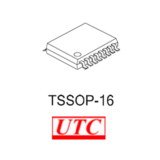
| 封裝/外殼 | TSSOP-16 |
| 安裝類型 | SMD 表面黏著式 |
| 無鉛狀態 RoHS | RoHS / Halogen free |
文件:U74HC4094.png)
U74HC4094 CMOS IC
8-STAGE SHIFT & STORE BUS REGISTER
DESCRIPTION
The U74HC4094 consists of an 8-stage shift register and an 8-stage D-type latch with 3-stage parallel outputs. Data is shifted serially through the shift register on the positive-going clock transition of the input singal. The output of the last stage QS1 can
be used to cascade several devices. The output of QS1 is transferred to a second output(QS2) on the following negative-going clock transition of the input singal.
The data of each stage of the shift register is provided with a latch whose data on the negative going transition of the Strobe input signal. When the strobe input is held high, data propagates through the latch to a 3-state output buffer.
The buffer is enabled when Output Enable input is taken high.
FEATURES
U74HC4094 CMOS IC
8段位移和存儲總線寄存器
描述
U74HC4094 包含一個8段位移寄存器和一個帶有3級並行輸出的8段D類型閘鎖存器。數據通過輸入信號的正跳沿在位移寄存器中進行串行位移。最後一級的輸出QS1可以用於級聯多個器件。在輸入信號的負跳沿之後,QS1的輸出被傳輸到第二個輸出(QS2)。
位移寄存器的每個段的數據具有鎖存器,在Strobe輸入信號的負跳沿時鎖存器的數據被提供。當Strobe輸入保持高電平時,數據通過鎖存器傳播到3狀態輸出緩衝器。
當輸出使能輸入信號變為高電平時,緩衝器被啟用。
特點
U74HC4094 CMOS IC
8-STAGE SHIFT & STORE BUS REGISTER
DESCRIPTION
The U74HC4094 consists of an 8-stage shift register and an 8-stage D-type latch with 3-stage parallel outputs. Data is shifted serially through the shift register on the positive-going clock transition of the input singal. The output of the last stage QS1 can
be used to cascade several devices. The output of QS1 is transferred to a second output(QS2) on the following negative-going clock transition of the input singal.
The data of each stage of the shift register is provided with a latch whose data on the negative going transition of the Strobe input signal. When the strobe input is held high, data propagates through the latch to a 3-state output buffer.
The buffer is enabled when Output Enable input is taken high.
FEATURES
- Operate from 2.0V to 6.0V
- Low Power Dissipation ICC=4μA(Max)
- High Noise Immunity Characteristic of CMOS Devices
U74HC4094 CMOS IC
8段位移和存儲總線寄存器
描述
U74HC4094 包含一個8段位移寄存器和一個帶有3級並行輸出的8段D類型閘鎖存器。數據通過輸入信號的正跳沿在位移寄存器中進行串行位移。最後一級的輸出QS1可以用於級聯多個器件。在輸入信號的負跳沿之後,QS1的輸出被傳輸到第二個輸出(QS2)。
位移寄存器的每個段的數據具有鎖存器,在Strobe輸入信號的負跳沿時鎖存器的數據被提供。當Strobe輸入保持高電平時,數據通過鎖存器傳播到3狀態輸出緩衝器。
當輸出使能輸入信號變為高電平時,緩衝器被啟用。
特點
- 工作電壓範圍:2.0V至6.0V
- 低功耗 ICC=4μA(Max)
- CMOS器件的高噪音免疫特性